Application Specific Integrated Circuit (ASIC) Floorplan Automation - Part I

MakinaRocks’ Combinatorial Optimization Problem (COP) team is working on a floorplan automation project, which automates component placement on Application-Specific Integrated Circuits (ASICs). In this post, we will provide a summary of the concept of floorplan automation in the semiconductor industry, outline the challenges the COP team is presently addressing, detail the strategies employed to tackle these issues, as well as the results obtained thus far. In the next post, we will address how our COP team has been solving the problem in greater detail.
Related to
- Reinforcement learning, taking on the challenges of the industry! - ASIC semiconductor design (Floorplan) automation (Naver Deview 21 presentation video)
- ASIC-Chip-Placement Part 2
1. ASIC Design
This chapter discusses ASIC, its design process, the placement of the floorplan within the process, and the importance of floorplan automation.
1.1 What is ASIC
To begin with, let’s define the fundamental concepts of ASIC. ASIC, an abbreviation for Application-Specific Integrated Circuit, is a custom-made semiconductor designed for applications in products like home appliances, mobile phones, and automobiles. In general, ASIC design aims to achieve low power consumption (Power), high speed (Performance), and high density (Area) to meet order specifications and requirements.
1.2 ASIC Design Flow
The ASIC design process consists of three stages: System-Level Design, Logic Design, and Physical Design.
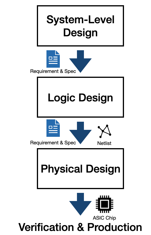
The system-level design defines the functions of the ASIC as well as ASIC specification such as power, timing and area.
A netlist that meets the required standards is developed in the subsequent logic design step. A netlist is a collection of nets. Each net delineates the connectivity among electronic components in circuit.
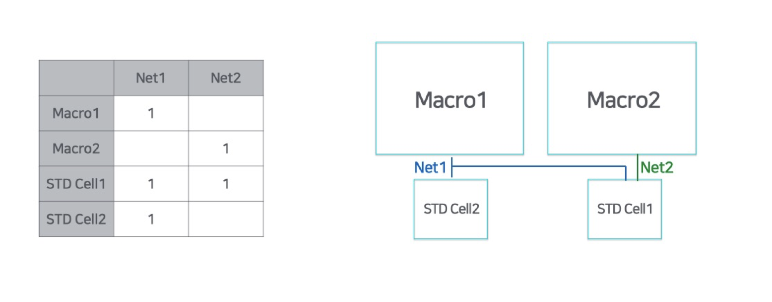
The electronic components can be categorized into relatively large-sized, known as macros, and the smaller-sized, referred to as standard cells. Macros are components created specifically for large-sized blocks of circuits that include processing units, SRAM, and more. standard cells are pre-built logic components that can be used to speed up the design process. Standard Cells, which are substantially smaller and more frequently used than macros, contain logic gate such as AND and OR.
Finally, in the physical design stage, the components are arranged in accordance with the netlist.
1.3 Physical Design
The physical design stage arranges the components on the empty chip canvas and connects the wires by the netlist and macro placement guidelines.
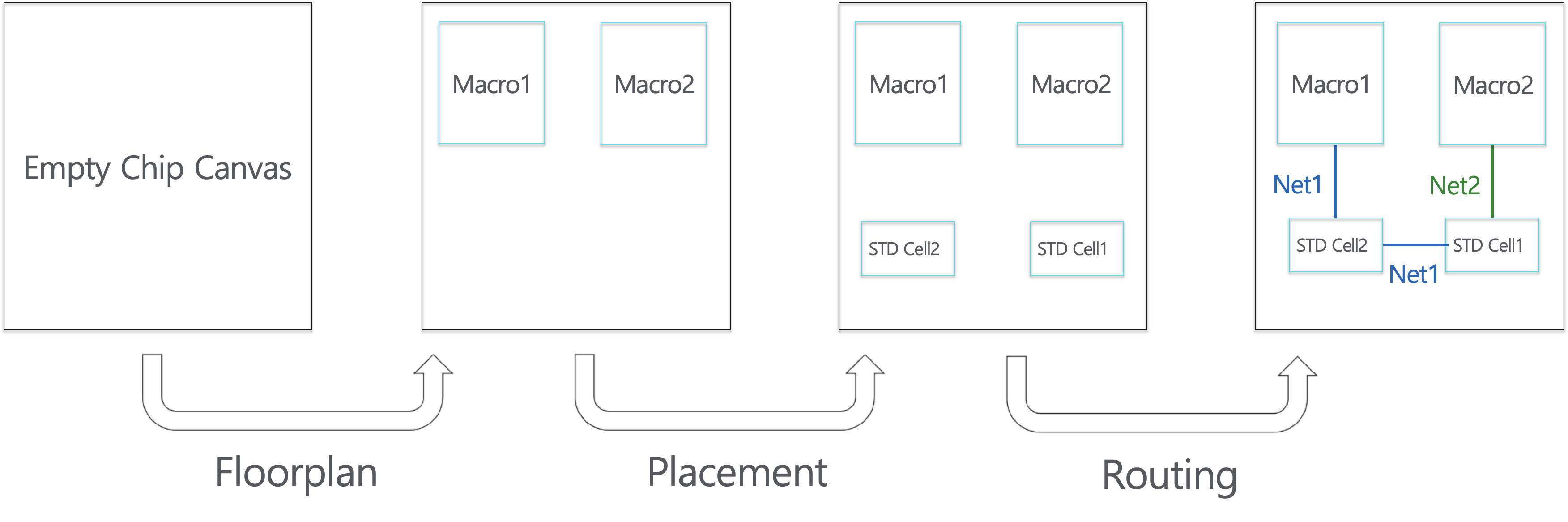
A chip canvas is a board on which components and wires are connected to form an electronic circuit. Physical design is primarily composed of the floorplan, placement, and routing stages.
During the floorplan stage, macros are placed on the empty chip canvas, while standard cells are placed during the placement stage. The components are physically connected to the chip canvas with wires during the routing stage.
Macros are placed earlier in the physical design than other standard cells, a phase we refer to as floorplan, due to their substantial space requirements on the chip canvas and potential placement restrictions.
This physical design stage can be aided by an Electronic Design Automation (EDA) tool, which automates the placement and routing stages. An example of an EDA tool is Synopsys ICC2 (Integrated Circuits Compiler 2), one of the most widely used programs. However, it is well-known that such an EDA tool does not guarantee optimal floorplan performance, so it is often carried out manually by semiconductor design professionals.
Our team has been working on developing a new floorplan automation procedure that ensures significantly improved performance compared to manual work, thus alleviating the challenges faced by semiconductor design experts.
1.4 Metric Determining Good Design
So, what metrics can be used to evaluate the efficacy of a floorplan?
Power, Performance, and Area (PPA) are the three most commonly used metrics for assessing the quality of a floorplan. In general, shorter wire lengths lead to higher PPA. Reduced wire lengths result in faster electric signal transmission, which improves performance, and reduces power consumption. Additionally, positioning components closely together enhances integration and minimizes the space they occupy on the canvas.
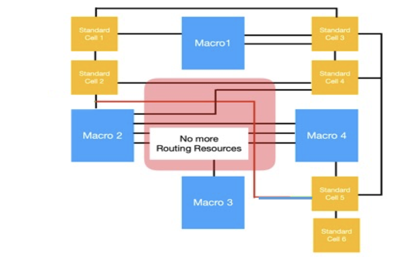
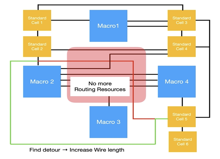
Placing components close together reduces the length of wires between them. Nevertheless, since routing resources on the chip, such as wire, are limited, simply positioning all wire-connected components arbitrarily close togheter does not guarantee shorter wire length and improved performance.
In Figure 4 on the left, we can see an example of using all routing resources in the red square area. Let’s consider connecting wires for Macro 2, Standard Cell 2, and Standard Cell 5. The red line represents the wire that connects these three components in the shortest path possible. However, because the wire has exhausted all routing resources, we can no longer place them within the red square area. Consequently, we must connect the wire by bypassing it, as shown in the figure on the right with the green line.
Violation is defined as the excessive utilization of routing resources, as illustrated in the figure below. When a violation occurs, no further wires can be installed in that area, and the wires must be routed through bypasses. Even when components are placed closely together, the wire length may become substantial due to limited routing resources.
A good floorplan necessitates an ‘optimal configuration,’ which involves allocating components within the smallest possible space while avoiding violations.
1.5 Floorplan Is Difficult
Finding the ‘optimal position’ for the components, on the other hand, is a challenging issue. The number of macros in an ASIC can range from tens to hundreds, while the overall number of components can range from hundreds of thousands to millions. A semiconductor design professional must analyze millions of connections for tens to hundreds of macros to determine the ‘optimal position’ of each macro.
Furthermore, the feedback process of the results placed by semiconductor design experts is time-consuming. The design process that follows the floorplan could take several days. When the quality of the final design is deemed insufficient, the floorplan procedure must be repeated.
Meanwhile, because floorplan relies on the expertise and experience of design engineers, the time spent and the quality of the design are highly dependent on the expertise of semiconductor design experts. This makes scheduling an entire semiconductor design process challenging.
1.6 Significance of the Problem Solution
We conducted a survey among engineers working in semiconductor design companies, encompassing both logic designers and physical designers, to gather their collective opinions on floorplan automation tools. Our findings revealed that several respondents, particularly among logic designers, found these automation tools to be valuable in providing clear and effective macro placement guidelines. Additionally, there was a shared sentiment among physical designers that these tools have the potential to streamline the floorplanning process, ultimately reducing the variability in design quality attributed to varying levels of expertise among engineers. Moreover, the consensus among all survey participants was that these automation tools significantly aid in meeting challenging semiconductor design schedules.
2. Previous Research, Recent Trends
2.1 Previous Research
Currently, implemented floorplan automation tools primarily employ meta-heuristic methods. In general, a meta-heuristic technique is a type of heuristic method that can be applied to numerous problems, irrespective of the problem’s nature. Some examples of meta-heuristic approaches to nonlinear optimization problems include Genetic Algorithms [1], Simulated Annealing [2], etc.
These meta-heuristic algorithms tend to work well and efficiently when dealing with small-sized problems. However, as problem sizes grow, the time required to compute solution grows exponentially, as do the difficulties in determining when the solution converges close to the optimum. Furthermore, problem-solving using this approach is inefficient in cases where we need to determine the floorplan for designs with minor differences because even a minor change in the logic design necessitates specifying and solving the entire placement as a new problem within the meta-heuristic approach.
2.2 Floorplan Using Reinforcement Learning
In recent years, there has been a notable shift in addressing the floorplan problem using machine learning approaches that train neural networks to create optimal layouts [3][4]. These machine learning techniques have the advantage of delivering strong performance even with minimal or no prior knowledge from a new netlist. Consequently, when training is complete, it leads to the rapid attainment of favorable results.
Reinforcement learning is one of the machine learning strategies that improves performance by using feedback to evaluate suboptimal results. Among these techniques, reinforcement learning is particularly suitable for addressing floorplan problems. This makes it especially well-suited for situations where defining an ‘optimal’ floorplan remains uncertain. As a result, there has been a growing body of research papers exploring the application of reinforcement learning to address floorplan challenges.
In our quest to advance floorplan automation, we’ve also explored the application of a novel reinforcement learning strategy.
3. What Do we Do?
3.1 Problem Definition
The COP team is solving the floorplan automation problem for a given netlist.
The netlist size was determined through consultation with current ASICLAND Design House employees. With a netlist of 1 million components, we set the complexity problem that the industry considers significant. And, in order to solve this problem, we are taking a step-by-step approach based on the number of components.
· Toy Example: 237 components
· Low complexity problem: 122,424 components
· Medium complexity problems: 633,339 components
· High complexity problem: Approximately 1,000,000 components
Performance is used as the evaluation metric. The Area is predetermined based on the requirements. Power is assessed at the end of the design process, allowing us to compare it with the front-end performance, similar to how physical designers evaluate it.
We use timing metrics like Worst Negative Slack (WNS) and frequency to evaluate Performance. When a signal is provided to each component, slack refers to the time difference between the required arrival time and the actual arrival time. The abbreviation for the minimum slack is WNS. If the WNS is less than 0,it violates the needed restriction. Thus, WNS must be at least 0.
\[\text{WNS} = \min_{v\in node}(\text{Required Arrival Time}(v) - \text{Actual Arrival Time}(v))\]The number of signals that can be processed per second, or the operation speed, is referred to as frequency. It is preferable to have a higher frequency.
In summary, the problem can be defined as:
The problem of finding macro placement of a WNS with zero or more and a maximum frequency for a given netlist.
In this post, we will provide the experimental results for the low-complexity challenge. A low complexity problem is relatively simple, making meaningful performance comparisons difficult. However, by solving the low-complexity problem, we demonstrated the feasibility of the Placer we designed, demonstrating the ability to solve medium- and high-complexity problems.
3.2 Method
Placer developed by the COP team is as follows.
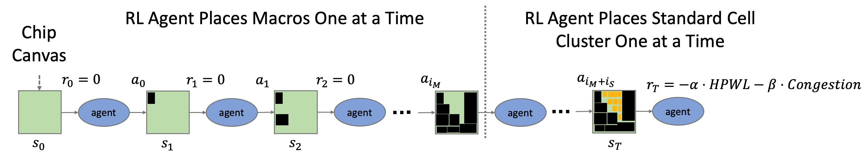
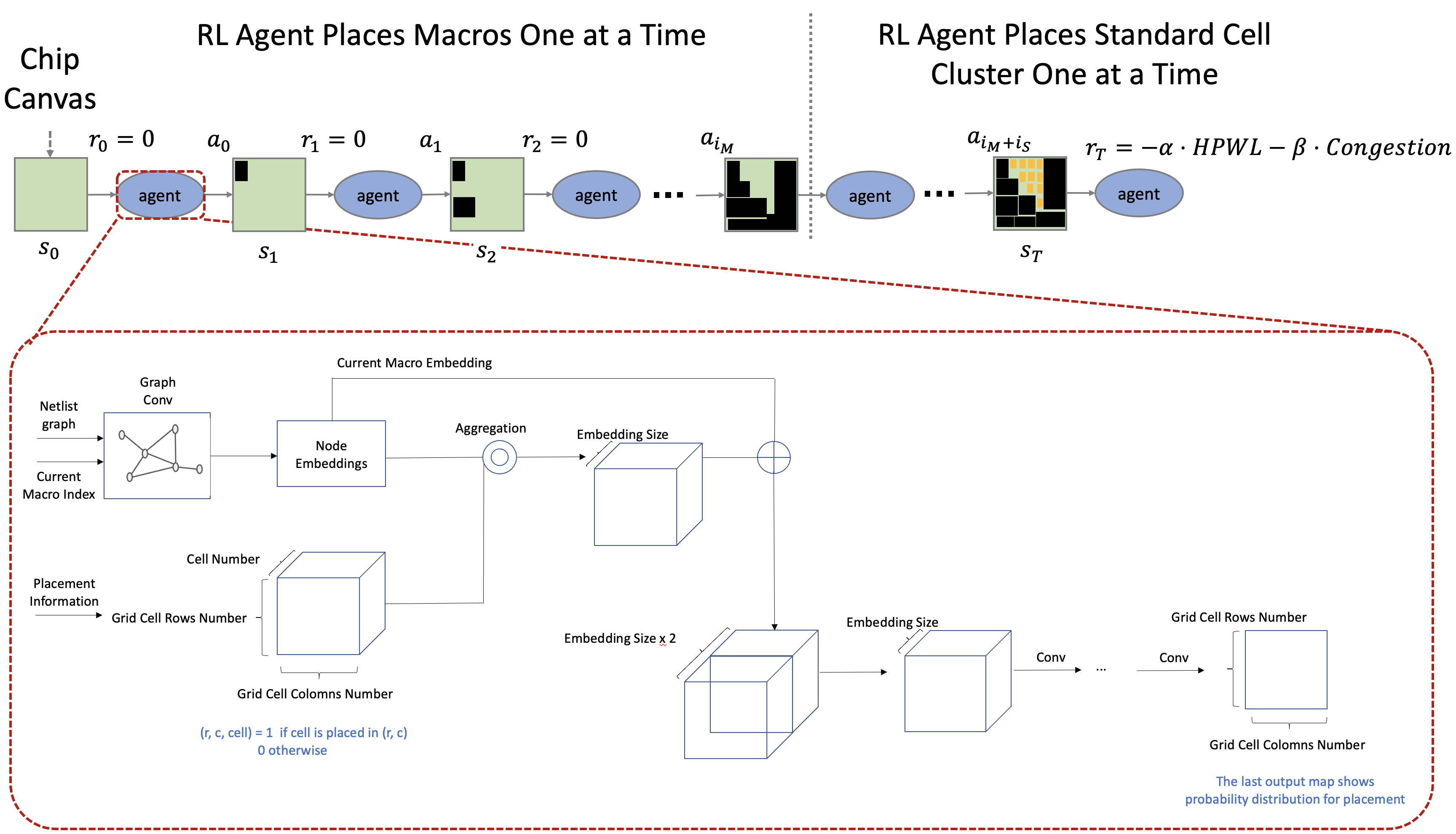
Because there are approximately 120,000 components to place, it is difficult to place all of them one by one using reinforcement learning. As a result, clustering standard cells and treating each cluster as a single component reduces the size of the problem.
After clustering, the neural network is used to embed the connection relationship information between the components in the netlist and the placement information of the components displayed on the canvas. Based on the value from the embedding, the reinforcement learning agent decides where to place the next component. The neural network learns by computing reward after the last component is placed. The macro placement information with the highest reward is produced at the end of the learning process.
The learning outcomes are verified using the workflow of actual semiconductor designers. When semiconductor design experts assess the functionality of floorplan, they do so after executing placement optimization, which readjusts the placement of components after they’ve been placed for reasons such as time. If there are no more violations and reasonable findings from WNS and Frequency are obtained, then proceed with the next procedure. If this is not the case, the floorplan process will be repeated. After performing placement optimization, we evaluated the floorplan by measuring WNS and frequency.
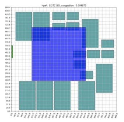
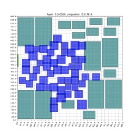
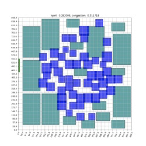
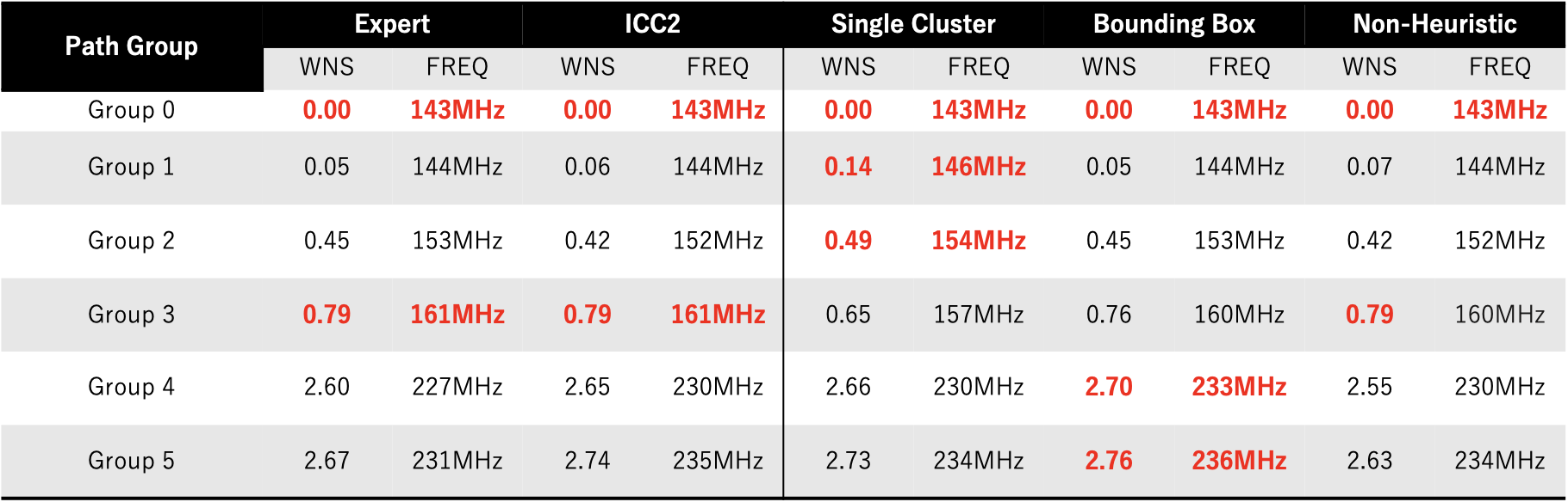
3.3 Experiment Result
-
Because the strong connectivity among standard cells, we could detect a tendency to position the standard cell in the middle of the canvas and the macro on the outside of the canvas when examining the semiconductor design expert’s floorplan progress at design house.
The first scenario places constraints on the placement of macros and standard cells based on these observations. We gradually increased the difficulty of learning in subsequent scenarios by removing constraints one by one.
- Single Cluster + Bounding Box: In the first scenario, the standard cells are clustered in the center, and the macros are restricted to the edge area, except for the input/output ports.
- Multiple Clusters + Bounding Box: In the second scenario, the standard cells are represented as multiple clusters, rather than as a single cluster as in the first scenario. The reinforcement learning agent places the cluster one by one. In addition, by allocating separate placement areas for standard cell and macro, macro can only be placed in the center and standard cell can be placed across the entire canvas area.
- Non-Heuristic: In the third scenario, the reinforcement learning agent places macros and standard cells throughout the canvas area without using any special heuristics.
With a semiconductor design expert at design house, the created placer was compared to the macro auto placement function, which automatically put macros in the ICC2 tool. The reinforcement learning placer performed similarly to the semiconductor design expert and the macro auto placement function.
4. Conclusion
We confirmed whether the placer that we developed performs well for netlists of low complexity. In the future, we hope to address the issue of floorplan automation in netlists of 600,000 cells, 1 million sizes, and more. We aim to solve placement problems for new Netlists with minimal additional learning.
Furthermore, we intend to extend and apply the technology related to reinforcement learning and combinatorial optimization problems discovered while solving the Floorplan problem to other types of combinatorial optimization problems, such as logistics base optimization and production facility optimization.
In this post, we discussed why floorplan automation is required during the ASIC design process. In addition, we introduced our COP team and how far they have progressed in solving the floorplan automation problem. In the following post, we will go over how the COP team solved the Floorplan automation problem in greater detail.
Reference
[1] Henrik Esbensen, 1992, A Genetic Algorithm for Macro Cell Placement.
[2] S. Kirkpatrick, C. D. Gelatt, Jr., M. P. Vecchi, 1983, Optimization by Simulated Annealing.
[3] Azalia Mirhoseini, Anna Goldie, Mustafa Yazgan, Joe Jiang, Ebrahim Songhori, Shen Wang, Young-Joon Lee, Eric Johnson, Omkar Pathak, Sungmin Bae, Azade Nazi, Jiwoo Pak, Andy Tong, Kavya Srinivasa, William Hang, Emre Tuncer, Anand Babu, Quoc V. Le, James Laudon, Richard Ho, Roger Carpenter, Jeff Dean, 2021, A graph placement methodology for fast chip design.
[4] Google AI, 2020, Chip Placement with Deep Reinforcement Learning, Google AI Blog.
Explore more
주문형 반도체 (ASIC) Floorplan 자동화 - Part III
Related to 강화학습, 산업의 난제에 도전하다! - ASIC 반도체 설계 (Floorplan) 자동화 (Naver Deview 21 발표 영상) ASIC-Chip-Placement 1부 ASIC-Chip-Placement...

Comments